Lab Introduction
Members' Pages
Principal Investigator
Research Professor
Ph.D. Students
M.S. Students
Undergraduate Students
- Eunseo Hong
- Ramyun Lee
A Compound semiconductor is a semiconductor compound composed of elements from two or more different groups of the periodic table. blah blah
Thru-hole epitaxy has recently been reported to be able to grow readily detachable domains crystallographically aligned with the underlying substrate over 2D mask material transferred onto a substrate. [Jang \textit{et al.}, \textit{Adv. Mater. Interfaces}, \textbf{2023} \textit{10}, 4 2201406] While the experimental demonstration of thru-hole epitaxy of GaN over multiple stacks of h-BN was evident, the detailed mechanism of how small holes in each stack of h-BN survived as thru-holes during multiple stacking of h-BN was not intuitively clear. Here, we use Monte Carlo simulations to investigate the conditions under which holes in each stack of 2D mask layers can survive as thru-holes during multiple stacking. If holes are highly anisotropic in shape by connecting smaller holes in a particular direction, thru-holes can be maintained with a high survival rate per stack, establishing more epitaxial connectedness. Our work verifies and supports that thru-hole epitaxy is attributed to the epitaxial connectedness established by thru-holes surviving even through multiple stacks.
Controllable growth and facile transferability of a crystalline film with desired characteristics, acquired by tuning composition and crystallographic orientation, become highly demanded for advanced flexible devices. Here the desired crystallographic orientations and facile transferability of a crystalline film can be achieved by “thru-hole epitaxy” in a straightforward and undemanding manner with no limitation on the layer number and polarity of a 2D space layer and the surface characteristics. The crystallographic alignment can be established by the connectedness of the grown material to the substrate through a small net cross-sectional area of thru-holes, which also allows the straightforward detachment of the grown material. Thru-hole epitaxy can be adopted for the realization of advanced flexible devices on large scale with desired crystallographic orientation and facile transferability.

 download:


It is very important to understand the electronic structure of GaAs and GaSb for fabrication of electronic and optoelectronic devices. Recently, tenary compounds, GaAs1-xSbx began to attract much attention from researchers because they were synthesized and expected to be new materials for optoeletronic devices. For x = 1 and x = 0, there have been a lot of computational studies to investigate their structural, electronic and optical properties, but few studies for general cases. Moreover, it has been known that “regular” density functional calculations does not describe the correct electronic structures including underestimated band gap and incorrect band splitting. To resolve such issues, we consider spin-orbit coupling effects and GW corrections on GaAs1-xSbx with the composition of x = 0, 0.25, 0.5, 0.75, and 1. To calculate their band structures, we make use of maximally localized Wannier functions to interpolate GW quasiparticle band structures. Based on our GW calculations, we discuss the trend of band gaps at various high symmetric points in the Brillouin zone with the composition x.
We report the existence of latent order during core relaxation in the high-angle grain boundaries (GBs) of GaN films using atomic-resolution scanning transmission electron microscopy and ab initio density functional theory calculations. Core structures in the high-angle GBs are characterized by two pairs of Ga-N bonds located next to each other. The core type correlates strongly with the bond angle differences. We identify an order of core relaxation hidden in the high-angle GBs by further classifying the 5/7 atom cores into a stable 5/7 core (5/7(S)) and a metastable 5/7 core (5/7(M)). This core-type classification indicates that metastable cores can exist at real high-angle GBs under certain circumstances. Interestingly, 5/7(M) exhibits distinct defect states compared to 5/7(S), despite their similar atomic configurations. We investigate the reconstruction of defect states observed in 5/7(M) by analyzing the real-space wave functions. An inversion occurred between two localized states during the transition from 5/7(S) to 5/7(M). We suggest an inversion mechanism to explain the formation of new defect states in 5/7(M).

 download:


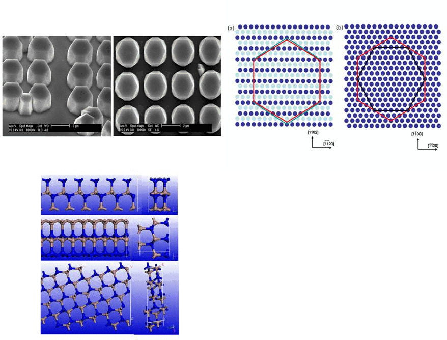
We have studied the growth and characterization of patterned and
uniformly distributed GaN microcrystals with well-defined facets and
epitaxy. The microcrystals were grown on a mask pattertned by
lithography, and formed by selective-area epitaxy using metal-organic
chemical vapour deposition. The GaN microcrystals have similar sizes
and shapes. Each microcrystal consists of an upper and lower part,
which are rotated by 30 deg. Transmission electron microscopy shows
that there is a rather clear interface between the two parts of the
crystal, suggesting a sudden change in the growth direction. We
performed ab initio calculations for the surface energies of
hexagonal GaN, and the growth morphology is explained based on surface
energy consideration.
 download:
