Table of Contents
van der Waals epitaxy of ZnO on hBN

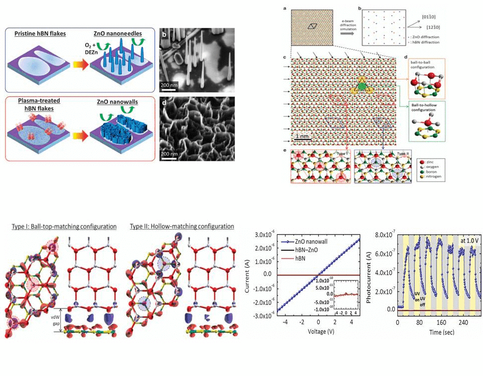
Integration of semiconductor on 2D atomic layers has offered flexible optoelectronic devices. Among various 2D atomic layers BN has great potentials for diverse device applications due to its excellent thermal conductivity and chemical stability as a wide-bandgap electric insulator. We found ZnO and BN were interacted through van der waals interaction using aberration-corrected high resolution transmission electron microscopy (HR-TEM) and ab initio calculations based on density function theory (DFT). We used DFT-D2 method of Grimme to describe London dispersion interactions.
- Architectured van der Waals epitaxy of ZnO nanostructures on hexagonal BN
Hongseok Oh, Young Joon Hong, Kun-Su Kim, Sangmoon Yoon, Hyeonjun Baek, Seoung-Hun Kang, Young-Kyun Kwon, Miyoung Kim, and Gyu-Chul Yi, NPG Asia Mater. 6, e145 (2014).
link:
 download:

