Table of Contents
Thru-hole epitaxy
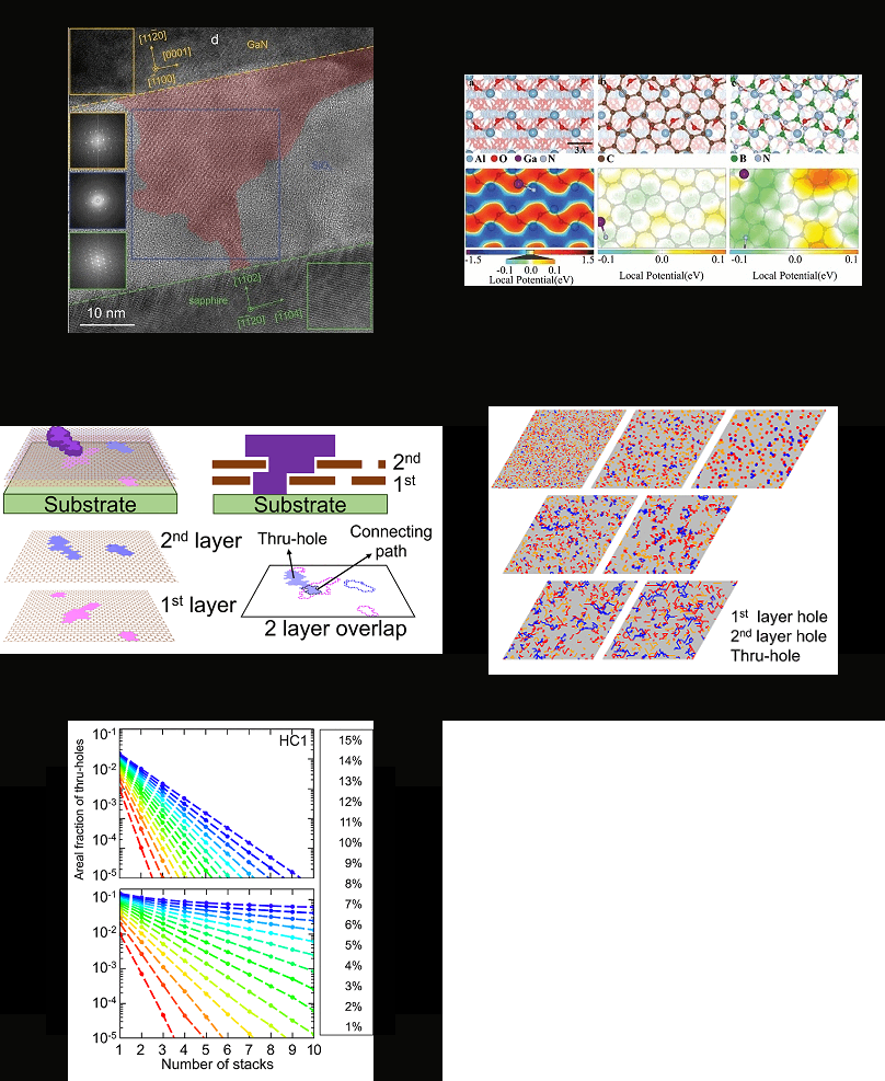
Thru-hole epitaxy has recently been reported to be able to grow readily detachable domains crystallographically aligned with the underlying substrate over 2D mask material transferred onto a substrate. [Jang \textit{et al.}, \textit{Adv. Mater. Interfaces}, \textbf{2023} \textit{10}, 4 2201406] While the experimental demonstration of thru-hole epitaxy of GaN over multiple stacks of h-BN was evident, the detailed mechanism of how small holes in each stack of h-BN survived as thru-holes during multiple stacking of h-BN was not intuitively clear. Here, we use Monte Carlo simulations to investigate the conditions under which holes in each stack of 2D mask layers can survive as thru-holes during multiple stacking. If holes are highly anisotropic in shape by connecting smaller holes in a particular direction, thru-holes can be maintained with a high survival rate per stack, establishing more epitaxial connectedness. Our work verifies and supports that thru-hole epitaxy is attributed to the epitaxial connectedness established by thru-holes surviving even through multiple stacks.
Controllable growth and facile transferability of a crystalline film with desired characteristics, acquired by tuning composition and crystallographic orientation, become highly demanded for advanced flexible devices. Here the desired crystallographic orientations and facile transferability of a crystalline film can be achieved by “thru-hole epitaxy” in a straightforward and undemanding manner with no limitation on the layer number and polarity of a 2D space layer and the surface characteristics. The crystallographic alignment can be established by the connectedness of the grown material to the substrate through a small net cross-sectional area of thru-holes, which also allows the straightforward detachment of the grown material. Thru-hole epitaxy can be adopted for the realization of advanced flexible devices on large scale with desired crystallographic orientation and facile transferability.
- Thru-hole Epitaxy: A Highway for Controllable and Transferable Epitaxial Growth
Dongsoo Jang, Chulwoo Ahn, Youngjun Lee, Seungjun Lee, Hyunkyu Lee, Donghoi Kim, Yongsun Kim, Ji-Yong Park, Young-Kyun Kwon, Jaewu Choi, and Chinkyo Kim, Adv. Mater. Interfaces, 10 (4), 2201406 (2023).
link:
 download:


