Table of Contents
Nanodevices
It is expected that the Moore's law would be broken in Si-based technology in the near future. To overcome this issue, we have performed research and development of various nanodevices based on nanostructured materials.
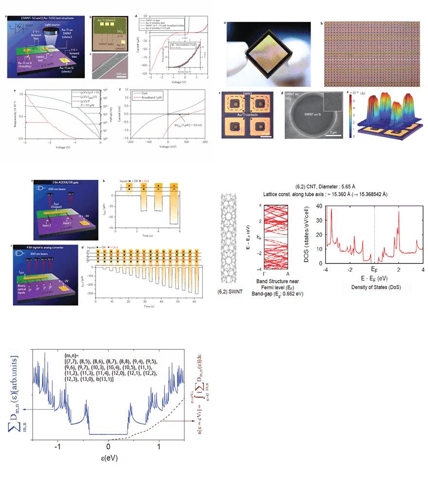
CNT-Si junctions-based optoelectronic devices

Recent progress in silicon photonics has dramatically advanced the
possible realization of heterogeneous logic circuits. A variety of
Boolean optoelectronic circuits have been proposed5. In this context,
experimental investigation of logic operations with both optical and
electrical inputs in chip-integrable devices is highly desirable.
Here, we present a new kind of photodiode-based logic device using
scalable heterojunctions of carbon nanotubes and silicon, the output
currents of which can be manipulated completely by both optical and
electrical inputs. This provides a novel platform for heterogeneous
optoelectronic logic elements with voltage-switchable photocurrent
responsivity of > 1 AW-1, photovoltage responsivity
of >1×10⁵ VW-1, electrical on/off ratios
of >1×10⁵ and optical on/off ratios of >1×10⁴.
To demonstrate their scalability, we fabricated a large array of
photoactive elements on a centimetre-scalewafer. We also present
bidirectional phototransistors and novel clock-triggerable logic
elements such as a mixed optoelectronic AND gate, a 2-bit
optoelectronic ADDER/OR gate and a 4-bit optoelectronic
digital-to-analog converter.
- Voltage-switchable photocurrents in single-wall carbon nanotube—silicon junctions for analogue and digital optoelectonics
Young Lae Kim, Hyun Young Jung, Sora Park, Bo Li, Fangze Liu, Ji Hao, Young-Kyun Kwon, Yung Joon Jung, and Swastik Kar, Nature Photon. 8 (3), 239-243 (2014).
link: download:


"Type-switchable" FETs based on CNTs and nanoparticles
We have reported the large-scale assembly of type-switchable field effect transistors (FETs) based on carbon nanotubes (CNTs) and nanoparticles (NPs). In this device, the charges stored in NPs adjacent to ambipolar CNT channels were adjusted to control the carrier type and density in the channels. We demonstrated the real-time reconfiguration of individual FET types and logic circuit functionality. Theoretical simulation of a model system was provided to explain this doping effect. This work takes advantage of the ambipolar properties of CNTs and opens up the possibility to build new types of devices with reconfigurable functionalities.
- Large-scale assembly of 'type-switchable' field effect transistors based on carbon nanotubes and nanoparticles
Sung Myung, Sungjong Woo, Jiwoon Im, Hyungwoo Lee, Yo-Sep Min, Young Kyun Kwon and Seunghun Hong, Nanotech. 21 (34), 345301 (2010).
link: download:


"Textured" network devices

Based on the percolation theory, we have performed device simulations
on network devices. We have found that it is possible to make
semiconducting devices out of mixture of metallic and semiconducting
nanotubes.
- "Textured" Network Devices: Overcoming Fundamental Limitations of Nanotube/Nanowire Network-based Devices
Minbaek Lee, Meg Noah, June Park, Maeng-Je Seong, Young-Kyun Kwon, and Seunghun Hong, Small 5 (14), 1642-1648 (2009).
link: download:


- Nanowire and nanotube transistors for lab-on-a-chip applications
Minbaek Lee, Ku Youn Baik, Meg Noah, Young-Kyun Kwon, Jeong-O Lee, Seunghun Hong, Lab Chip 9 (16), 2267-2280 (2009).
link: download:

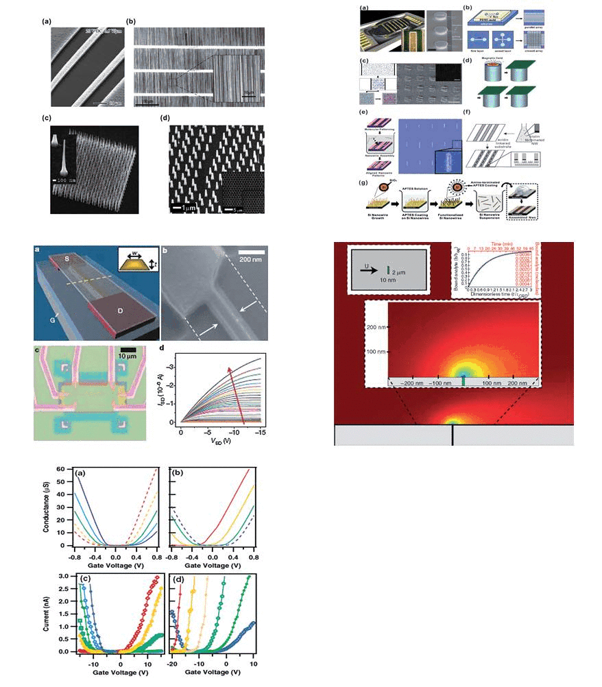
Linker-free directed assembly of high-performance integrated devices
dvanced electronic devices based on carbon nanotubes (NTs) and various types of nanowires (NWs) could have a role in next generation semiconductor architectures. However, the lack of a general fabrication method has held back the development of these devices for practical applications. Here we report an assembly strategy for devices based on NTs and NWs. Inert surface molecular patterns were used to direct the adsorption and alignment of NTs and NWs on bare surfaces to form device structures without the use of linker molecules. Substrate bias further enhanced the amount of NT and NW adsorption. Significantly, as all the processing steps can be performed with conventional microfabrication facilities, our method is readily accessible to the present semiconductor industry. We use this method to demonstrate large-scale assembly of NT- and NW-based integrated devices and their applications. We also provide extensive analysis regarding the reliability of the method.
- Linker-free directed assembly of high-performance integrated devices based on nanotubes and nanowires
M. Lee, J. Im, B.Y. Lee, S. Myung, J. Kang, L. Huang, Y.-K. Kwon, and S. Hong, Nature Nanotech. 1 (1), pp. 66-71 (2006).
link: download:


"Bucky-shuttle" memory device
We investigate the internal dynamics of a related model system, consisting of a K@C+60 endohedral complex enclosed in a C480 nanocapsule. We show this to be a tunable two-level system, where transitions between the two states can be induced by applying an electric field between the C480 end caps, and discuss its potential application as a nonvolatile memory element.
- "Bucky Shuttle" Memory Device: Synthetic Approach and Molecular Dynamics Simulations
Young-Kyun Kwon, David Tomanek, and Sumio Ijima, Phys. Rev. Lett. 82 (7), 1470-1473 (1999).
link: download:

- [Proceedings] The potential of carbon-based memory systems
Mark Brehob, Richard Enbody, Young-Kyun Kwon, and David Tomanek, in R. Rajsuman, and T. Wik (eds.), Memory Technology, Design and Testing, 1999. Records of the 1999 IEEE International Workshop on, pp. 110-114, IEEE Computer Society, San Jose, CA (1999).
link: download:

- [Patent] Nanocapsules Containing Charged Particles, their Uses and Methods of Forming the Same
David Tomanek, Richard J. Enbody, Young-Kyun Kwon and Mark Brehob, US Patent 6,473,351 issued on October 29, 2002.
link: download:
